
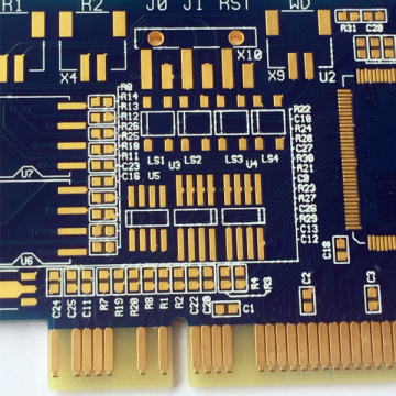
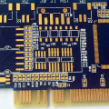
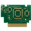
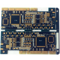
6-layer High Tg Leadless Gold Finger PCB
Basic Info
Model No.: 6 Layer Rigid PCB Polyimide
Product Description
What is PCB gold finger?
In High Quality Prototype PCB Fabrication, let's understand how to deal with gold fingers in 6 layer Rigid-flex Immersion Gold PCB and some details.
1. Electroplating nickel gold: the thickness can reach 3-50u", because of its superior conductivity, oxidation resistance and wear resistance, it is widely used in gold finger PCBs that require frequent insertion and removal or PCB boards that require frequent mechanical friction. Above, but because of the extremely high cost of gold plating, it is only used for partial gold plating such as gold fingers.
2. Immersion gold: the thickness is conventional 1u", up to 3u" because of its superior conductivity, flatness and solderability, it is widely used in high-precision PCB boards with button positions, bonded IC, BGA, etc. Gold finger PCBs with low wear resistance requirements can also choose the entire board immersion gold process, which is much lower than the electro-gold process cost. The color of the Immersion Gold process is golden yellow.
1) In order to increase the wear resistance of gold fingers, gold fingers usually need to be plated with hard gold.
2) The golden finger needs to be chamfered, usually 45°, other angles such as 20°, 30°, etc. If there is no chamfer in the design, there is a problem.
3) The gold finger needs to be treated as a whole piece of solder mask to open the window, and the PIN does not need to open the steel mesh;
4) Immersion tin and silver immersion pads need to be at a minimum distance of 14mil from the top of the finger; it is recommended that the pad is more than 1mm away from the finger position during design, including via pads;
5) Do not spread copper on the surface of the gold finger;
6) All layers of the inner layer of the gold finger need to be cut copper, usually the width of the cut copper is 3mm larger; it can be used for half-finger cut copper and entire finger cut copper.
The main function of the golden finger is to connect, so it must have good electrical conductivity, wear resistance, oxidation resistance, and corrosion resistance.
Because the texture of pure gold (gold) is relatively soft, gold fingers generally do not use gold, but only a layer of "hard gold (gold compound)" is electroplated on it, which can not only obtain good electrical conductivity of gold, but also make it resistant Abrasion performance, anti-oxidation performance.
So has the PCB used "soft gold"? The answer is of course there is use, such as the contact surface of some mobile phone buttons, COB (Chip On Board) with aluminum wire and so on. The use of soft gold is generally electroplating to deposit nickel gold on custom pcb fabrication, and its thickness control is more flexible.


Product Categories : 0-18Layer FR4 Board > 6 Layer Laser Circuits